Electrical properties of Germanium (Ge)

Electrical properties
Basic ParametersMobility and Hall Effect
Transport Properties in High Electric Fields
Impact Ionization
Recombination Parameters
Basic Parameters
| Breakdown field | ≈105V cm-1 |
| Mobility electrons | ≤3900 cm2 V-1s-1 |
| Mobility holes | ≤1900 cm2 V-1s-1 |
| Diffusion coefficient electrons | ≤100 cm2 s-1 |
| Diffusion coefficient holes | ≤50 cm2 s-1 |
| Electron thermal velocity | 3.1·105m s-1 |
| Hole thermal velocity | 1.9·105m s-1 |
Mobility and Hall Effect
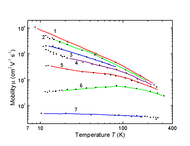 |
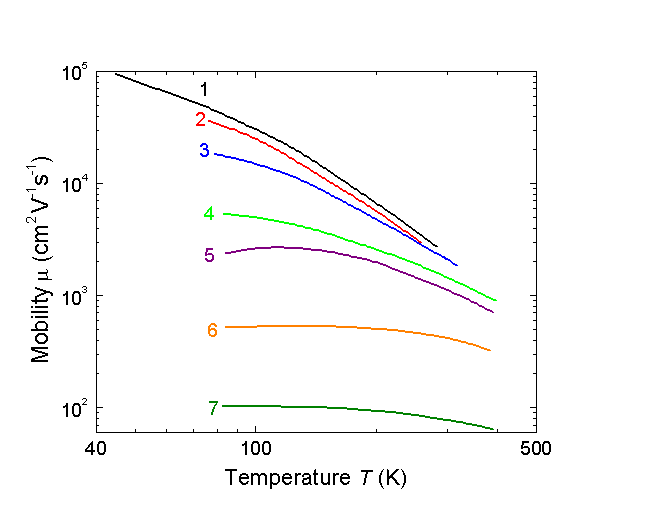
Electron mobility versus temperature for different doping levels. 1. High purity Ge; time-of-flight technique (Jacoboni et al. [1981]); 2-6. Hall effect Nd - Na(cm-3): 2. 1·1013; 3. 1.4·1014; 4. 1.7·1015; 5. 7.5·1015; 6. 5.5·1016 (Debye and Conwell [1954]); 7. Hall effect Nd - Na=1.2·1019(cm-3) (Fistul et al. [1962]). |
µn≈ 4.9·107·T-1.66 (cm2 V-1 s-1).
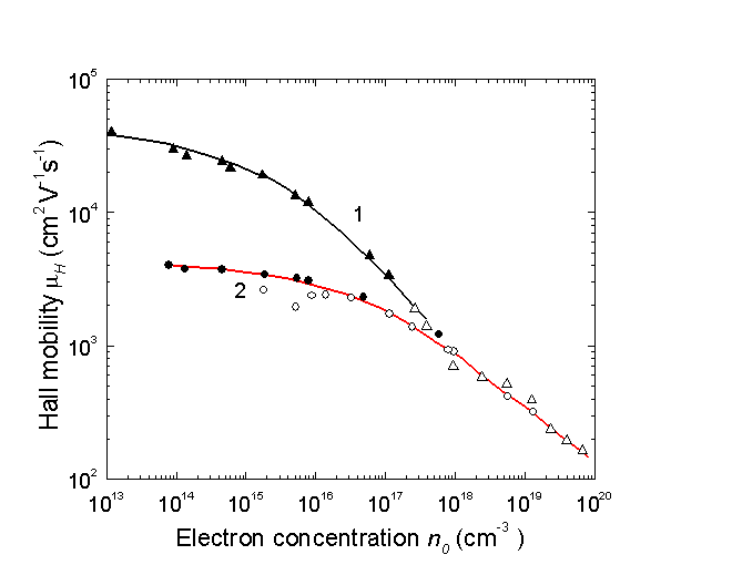 |
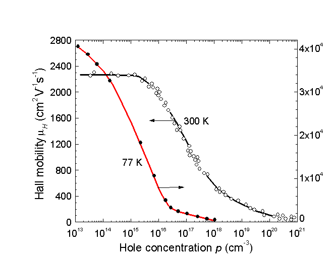
Electron Hall mobility versus electron concentration 1. T = 77 K; 2. T = 300 K. (Fistul et al. [1962]). |
Approximate formula for the Hall mobility. 300 K.
µn=µOH/(1+Nd·10-17)1/2,where µOH≈=3900 (cm2 V-1 s-1),
Nd- in cm-3
(Hilsum [1974]).
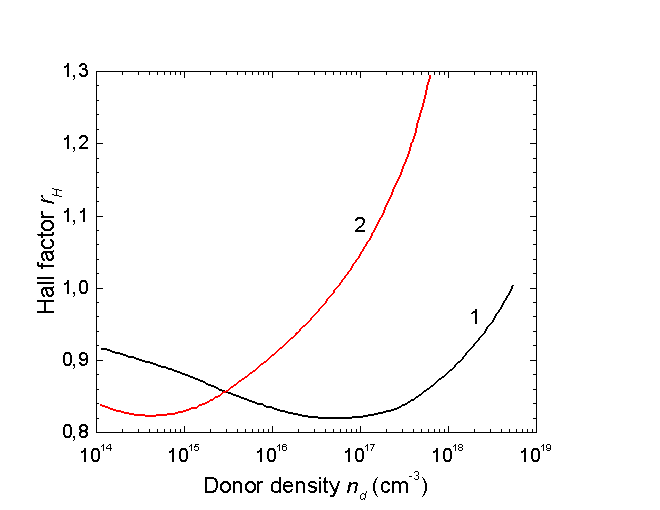 |
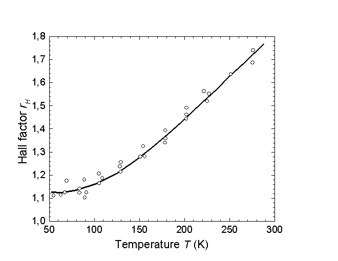
The electron Hall factor versus donor density. 1. T = 300 K; 2. T = 77 K. (Babich et al. [1969]). |
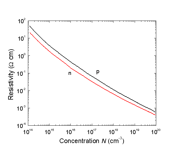 |
Resistivity versus impurity concentration., T = 300 K. (Cuttris [1981]). |
 |
Temperature dependences of hole mobility for different doping levels. 1. High purity Ge; time-of-flight technique (Ottaviany et al. [1973]). 2-7. Hall-effect (Golikova et al. [1961]). Na- Nd (cm-3): 2. = 4.9·1013; 3. 3.2·1015; 4. 2.7·1016; 5. 1.2·1017; 6. 4.9·1018; 7. 2.0·1020. |
µp≈1.05·109·T-2.33 (cm2 V-1 s-1)
 |
The hole Hall mobility versus hole concentration. Experimental points: data from three References (Golikova et al. [1961]). |
 |
The hole Hall factor versus temperature for high purity p-Ge (Morin [1954]). |
Transport Properties in High Electric Fields
 |
Ge. Electron drift velocity vs. electric field. Solid lines: F||(100) Solid lines: F||(111). Jacoboni et al. (1981). |
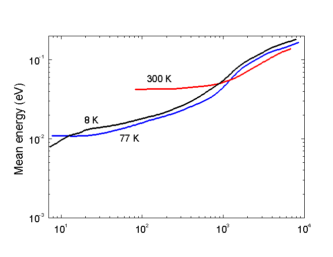 |
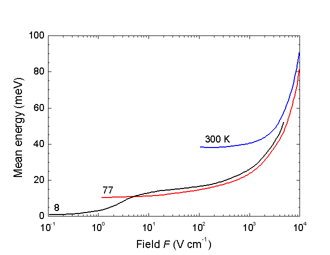
Ge. Mean energy of electrons in lower valleys vs. electronic field
for three lattice temperatures. (Jacoboni et al. [1981]). (Jacoboni et al. [1981]). |
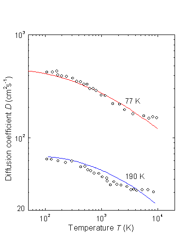 |
Ge. Longitudinal electron diffusion coefficient D vs. electric field
for 77 K and 190 K. F||(100). Solid lines show the results calculation. Symbols represent measured data. (Jacoboni et al. [1981]). |
 |
Ge. Electron drift velocity vs. electric field at different temperatures. F||(100). Ottaviani et al. (1973). |
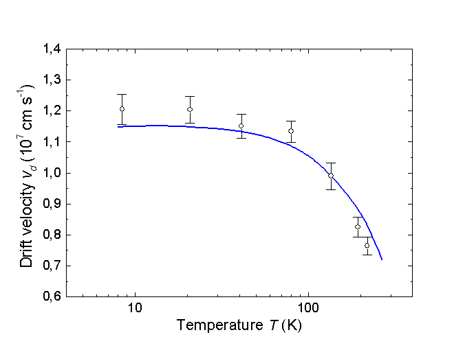 |
Ge. Drift velocity Vd vs. of temperature for electric field F=104(V cm-1). F||(100). Solid line show the results of calculation in the case where non-parabolic effect are taken into account (Reggiani et al. [1977]). |
 |
Ge. Mean energy of hole vs. electronic field F at different lattice
temperatures. Solid line are Monte-Carlo calculations for F||(111) (Reggiani et al. [1977]). Points show experimental results for 82 K. (Vorob'ev et al. [1978]). |
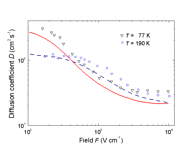 |
Ge. Longitudinal hole diffusion coefficient D vs. electronic
field for 77 K and 190 K. F||(111). Dashed and solid lines show the results of the calculations. Symbols represent measured data. (Reggiani et al. [1978]). |
Impact Ionization
There are two schools of thought regarding the impact ionization in Ge.The first one states that impact ionization rates αi and βi for electrons and holes in Ge are known accurately enough to distinguish such subtle details as the anisothropy of αi and βi for different crystallographic directions.
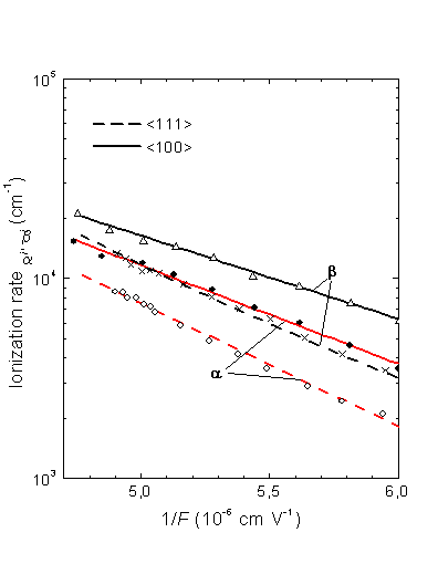 |
Ionization rates in (111) and (100) directions versus 1/F. T = 300 K. (Mikava et al. [1977]). |
| Remarks | Referens | |||
| Electron ionization rates | Ge (111) | αi = α0 x exp(-Ei
/E), where α0 = 2.72x10⁶ 1/cm, Ei = 1.1x10⁶ V/cm |
(111), 300 K | Mikava et al. (1980) |
| Ge (100) | αi = α0 x exp(-Ei
/E), where α0 = 8.04x10⁶ 1/cm, Ei = 1.4x10⁶ V/cm |
(100), 300 K | Mikava et al. (1980) | |
| Hole ionization rates | Ge (111) | βi = β0 x exp(-Ei
/E), where β0 = 1.72 x 10⁶ 1/cm, Ei = 9.37 x 10⁵ V/cm |
(111), 300 K | Mikava et al. (1980) |
| Ge (100) | βi = β0 x exp(-Ei
/E), where β0 = 6.39 x 10⁶ 1/cm, Ei = 1.27 x 10⁶ V/cm |
(100), 300 K | Mikava et al. (1980) |
The second school contends that the values of αi and βi for the same electric field reported by different researches differ by an order of magnitude. This point of view is explained by Kyuregyan and Yurkov [1989]. In accordance with this approach we can assume for all crystallographic directions that
| For electrons: αi=αoexp(-Fno/ F) | ||
| where | αo = 2.84·106 cm-1 | Fno = 1.14·106 V cm-1 |
| For holes: βi=βoexp(-Fpo/ F) | ||
| where | βo = 4.21·106 cm-1 | Fpo = 1.11·106 V cm-1 |
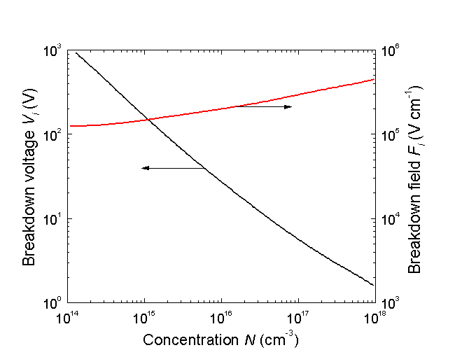 |
Breakdown voltage and breakdown field versus doping density for an abrupt p-n junction. (Kyuregyan and Yurkov [1989]). |
Recombination Parameters
| Pure n-type material | |
300 K |
|
| The longest lifetime of holes | τp≥ 10-3 s |
| Diffusion length | Lp≥ 0.2 cm |
77 K |
|
| The longest lifetime of holes | τp≥ 10-4 s |
| Diffusion length | Lp≥ 0.15 cm |
| Pure p-type material | |
300 K |
|
| The longest lifetime of electrons | τn≥ 10-3 s |
| Diffusion length | Ln≥ 0.3 cm |
77 K |
|
| The longest lifetime of electrons | τn≥ 10-4 s |
| Diffusion length | Ln≥ 0.15 cm |
| Surface recombination | 10 ÷ 106cm/s. |
| Radiative recombination coefficient at 300 K | 6.41·10-14 cm3 s-1 |
| Auger coefficient at 300 K | ~10-30 cm6 s-1 |
| SiGe | Remarks | Referens | ||
| The longest lifetime of holes tp | x 10-7 c | 300 K | ||
| Diffusion length Lp = (Dp x tp)1/2 | μm c | Surface Recombinaton Velocity | 1 | |
| Radiative recombination coefficient B | x 10-12 cm3/s | |||
| Auger coefficient Cn | x 10-31 cm6/s | |||
| Auger coefficient Cp | x 10-31 cm6/s | |||
| Auger coefficient C = Cn + Cp | x 10-31 cm6/s |