NSM Archive - Gallium Nitride (GaN) - Mobility and Hall Effect

Mobility and Hall Effect
Wurtzite GaN.
GaN is an extrinsic n-type semiconductor, p-type material does not seem achievable. Above room temperature transport is predominantly determined by polar-optical scattering and at lower temperatures by impurity scattering. Crystals with n larger than 8x1018cm-3 show metallic conduction with no appreciable variation in n or μn between 10 and 300 K.| Remarks | Referens | ||
| Conductivity σ | 6÷12 Ω-1 cm-1 | 300 K ; n ~= 1017 cm-3, undoped layers grown by vaporphase technique on sapphire | Ilegems (1972); Ilegems & Dingle (1973); Crouch et al. (1978) |
| Mobility electrons μn | =< 440 cm2 V-1 · s -1 | 300 K ; purest material, n ~= 1017 cm-3 | Ilegems (1972); Ilegems & Dingle (1973); Crouch et al. (1978) |
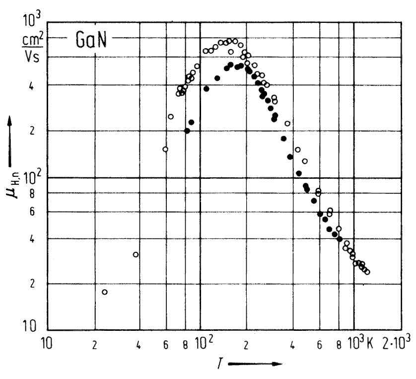 |
GaN, Wurtzite sructure. Electron Hall mobility vs. temperature for two samples Ilegems & Montgomery (1973). |
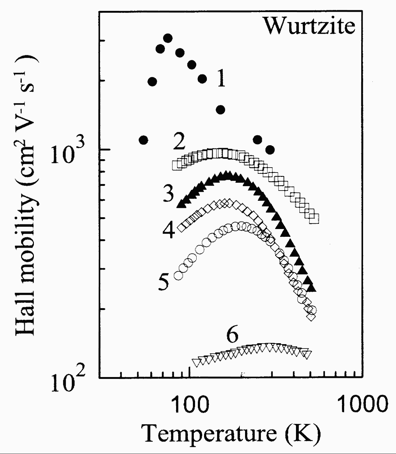 |
GaN, Wurtzite sructure. Electron Hall mobility versus temperature
for different doping levels and different degrees of compensation θ
= Na/Nd. 1 - unintentionally doped [Nakamuraetal.(1992)]; 2 - Nd = 3.1x 1017 cm-3, θ < 0.03 [Gotz et al. (1996)]; 3 - Nd = 1.1 x 1017cm-3, θ ~= 0.3 [Gotz et al. (1996)]; 4 - Nd = 2.3 x 1017 cm-3, θ < 0.04 [Gotz et al. (1996)]; 5 - Nd = 7.4 x 1017 cm-3, θ < 0.01 [Gotz et al. (1996)]; 6 - The concentration of introduced Si Ndo = 2 x 1019cm-3 [Gotz et al. (1996)]. The calculations of electron mobility vs. the temperature for different doping levels and compensation ratios see in Chin et al. (1994). |
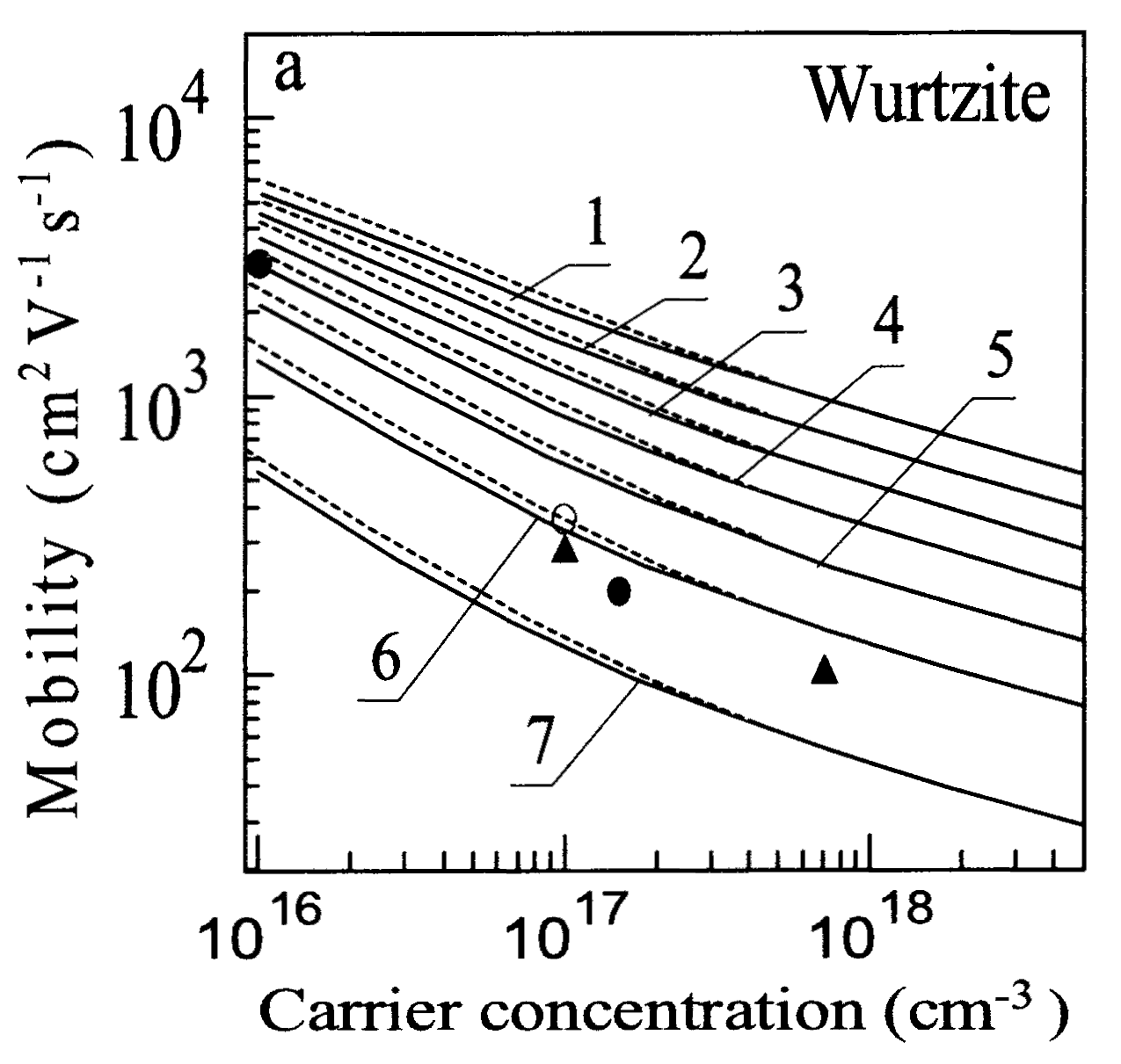 |
GaN, Wurtzite sructure. The calculated electron drift (solid
curves) and Hall (dashed curves) mobility versus carrier concentration
at different compensation ratios θ: 1 - θ = 0; 2 - θ = 0.15; 3 - θ = 0.30; 4 - θ = 0.45; 5 - θ = 0.60; 6 - θ = 0.75; 7 - θ = 0.90. T = 77 K. Experimental data are taken from four different papers Chin et al. (1994). |
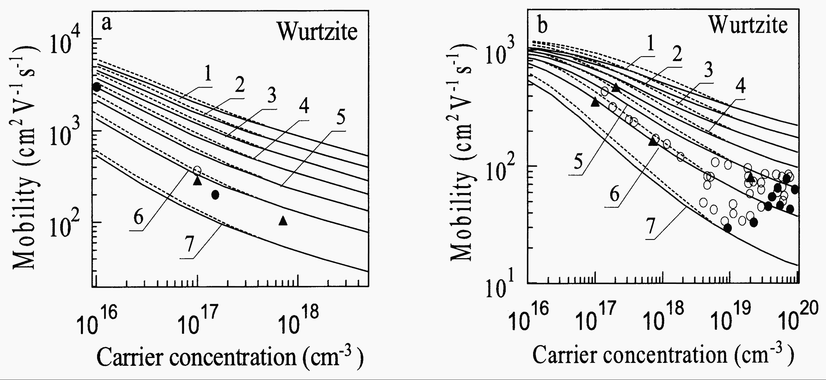 |
GaN, Wurtzite sructure. The calculated electron drift (solid
curves) and Hall (dashed curves) mobility versus carrier concentration
at different compensation ratios θ: 1 - θ = 0; 2 - θ = 0.15; 3 - θ = 0.30; 4 - θ = 0.45; 5 - θ = 0.60; 6 - θ = 0.75; 7 - θ = 0.90. T = 300K. Experimental data are taken from four different papers Chin et al. (1994). |
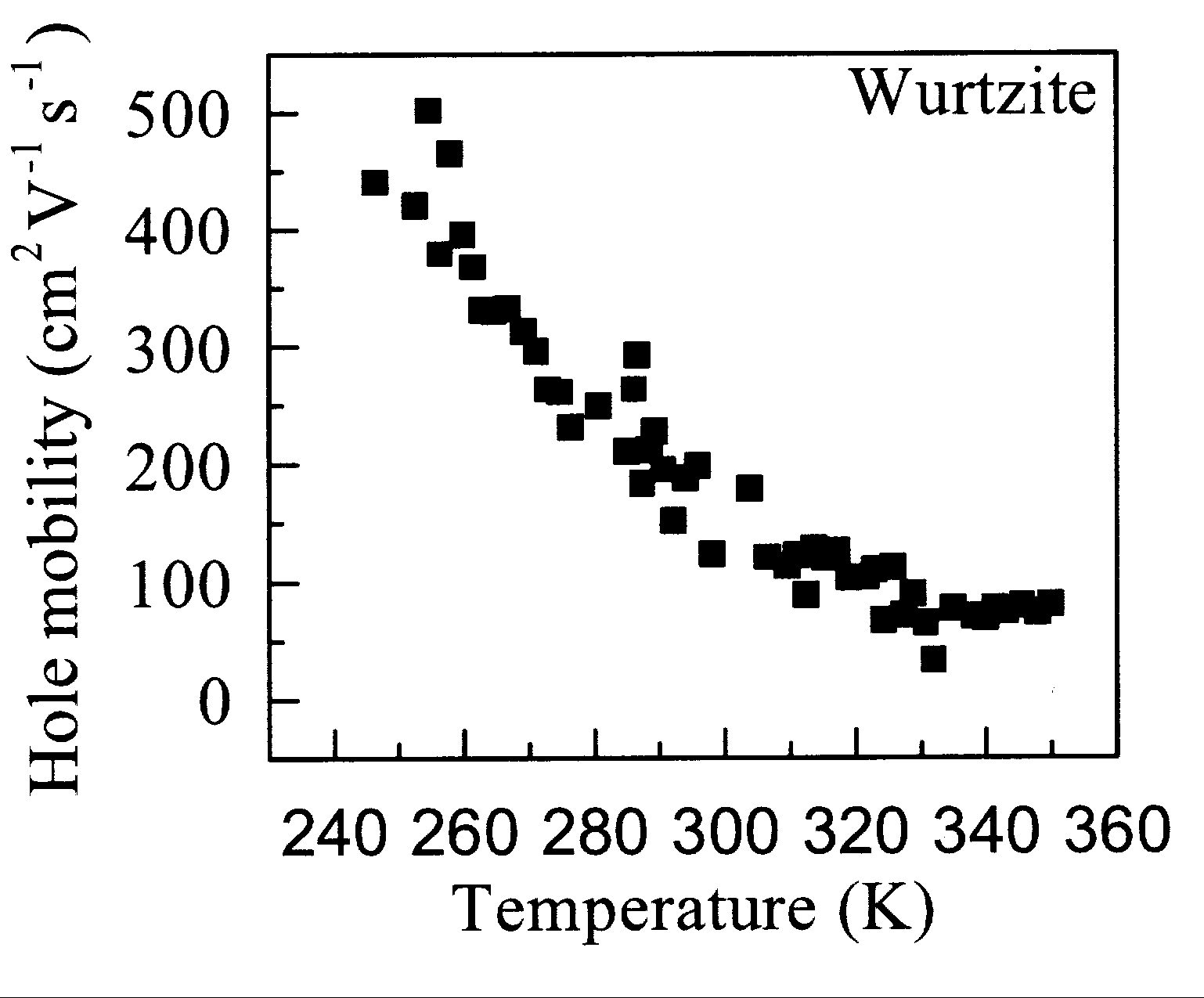 |
GaN, Wurtzite sructure. Hole Hall mobility versus temperature. Hole
concentration at T= 300 K and p ~= 4 x 1012 cm-3
Rubin et al. (1994). |
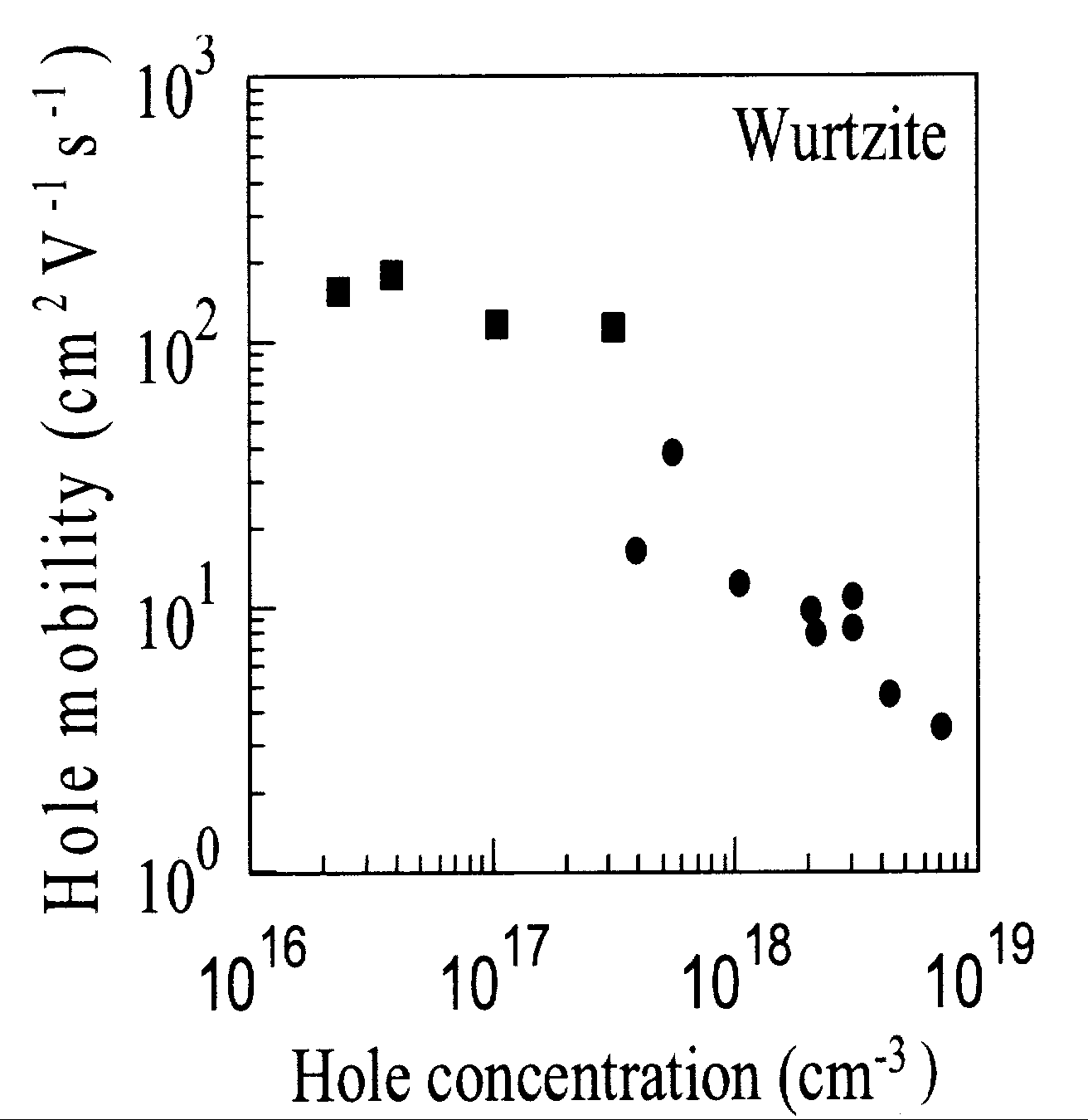 |
GaN, Wurtzite sructure. Hole Hall mobility versus hole concentration
GaN at T = 300 K Gaskill et al. (1995). |
Zinc Blende GaN (cubic)
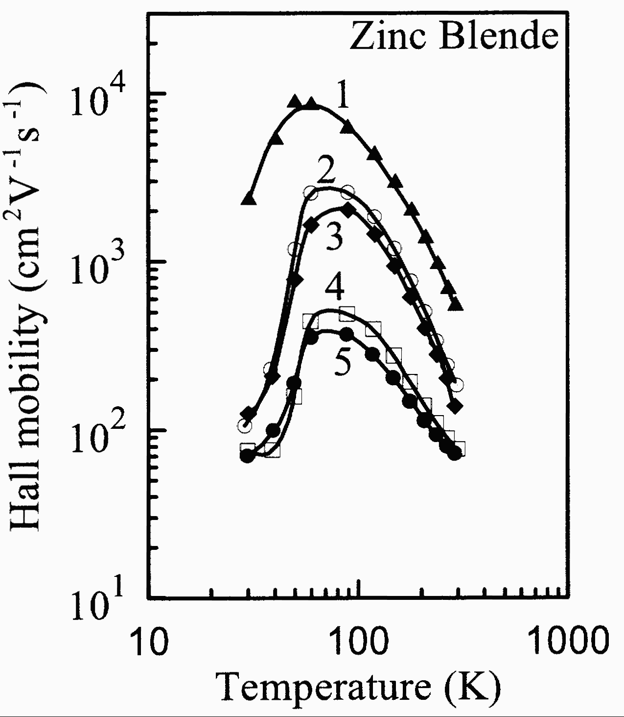 |
GaN, Zinc Blende (cubic). Electron Hall mobility versus temperature
for different doping levels (cubic GaN). Electron concentration at room temperature: 1 - 1.5 x 1018 cm-3; 2 - 1.3 x 1019 cm-3, 3 - 2.8 x 1019 cm-3; 4 - 1.5 x 1020 cm-3, 5 - 3 x 1020 cm-3. Kim et al. (1994). |
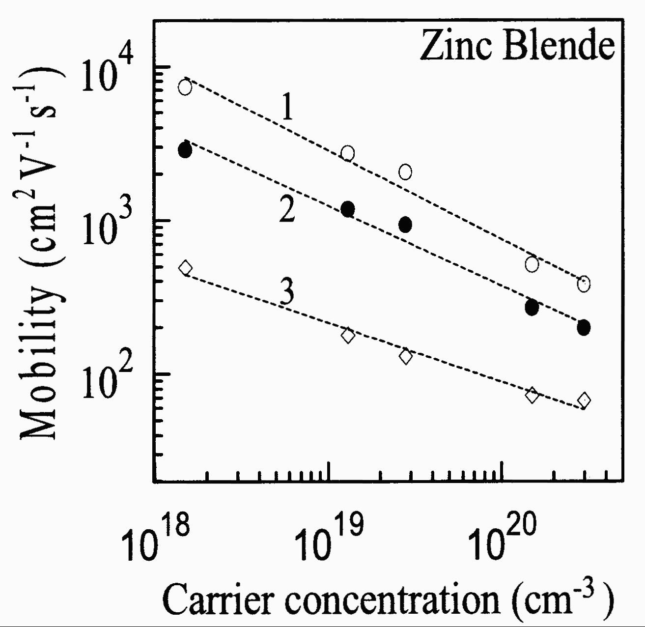 |
GaN, Zinc Blende (cubic). The electron Hall mobility at three
temperatures vs. the carrier concentration. T (K): 1-80; 2-150; 3-300. Kim et al. (1994). |
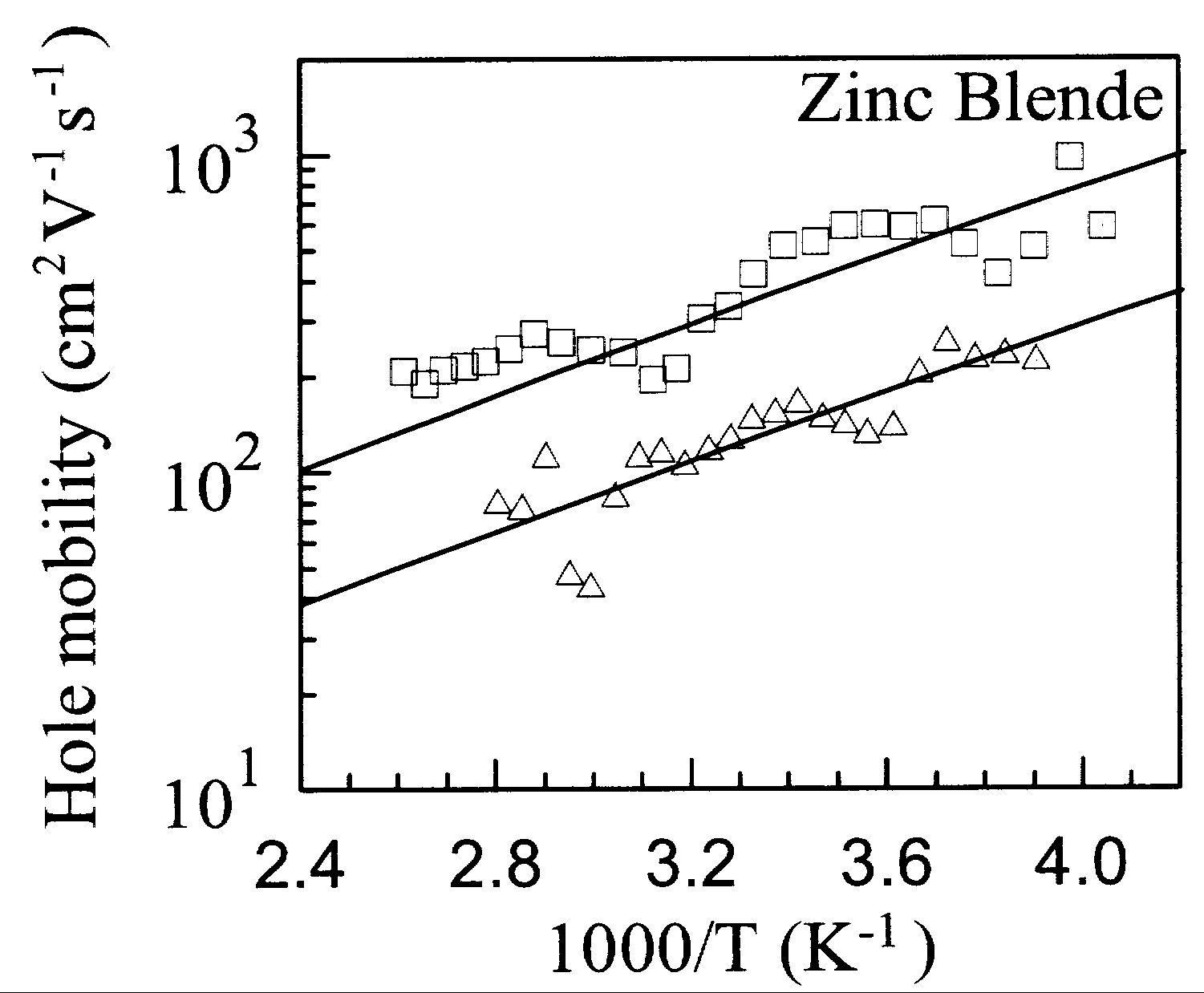 |
GaN, Zinc Blende sructure. The hole Hall mobility vs the temperature
(two samples). The hole concentration p = (0.6 - 1) x 1013
cm-3 at T= 300K . As et al. (1996). |
Two-Dimensional Electron Gas Mobility at AlGaN/GaN interface
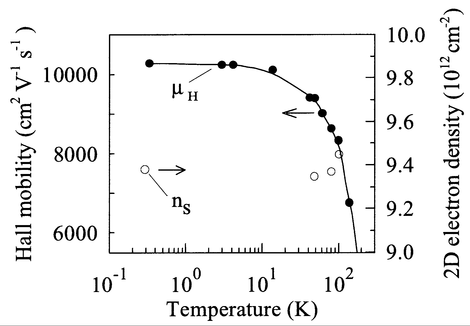 |
GaN. Electron Hall mobility and sheet concentration vs. temperature
for two-dimensional gas in AlGaN/GaN heterostructure grown on 6H-SiC substrate.(the
sample as in next Figure). Gaska et al. (1998). |
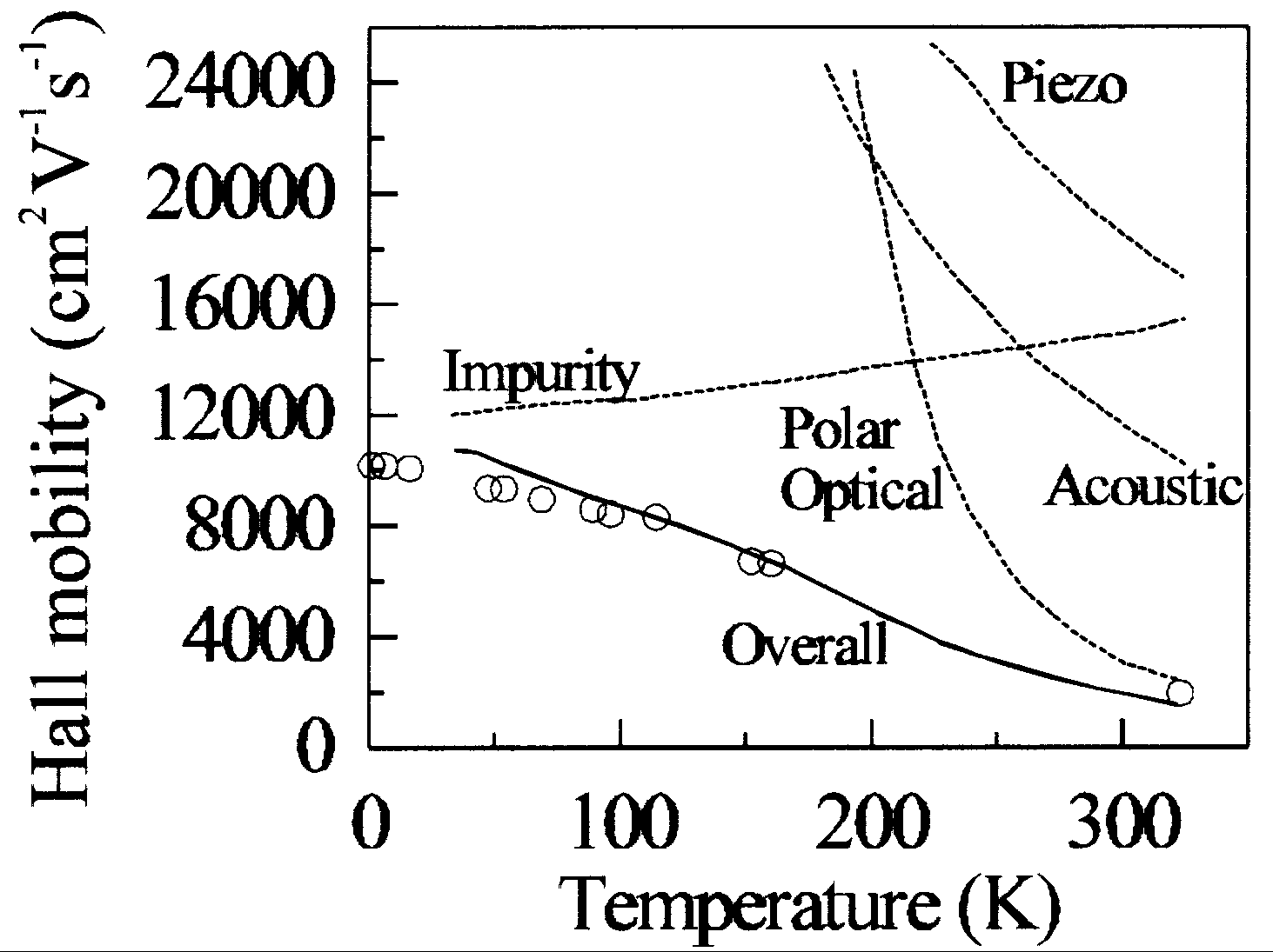 |
GaN. Measured (open circles) and calculated (solid lines)
Hall mobility versus temperature (the sample as in previous Figure).
Electron scattering processes by optical and acoustic phonons, piezoelectric,
and impurity scattering were taken into account. Gaska et al. (1998). |
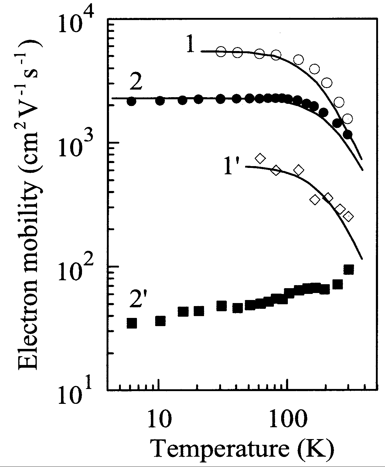 |
GaN. Electron Hall mobility versus temperature for two AlGaN/ GaN
heterostructures (1,2) and related GaN layers (1',2' ) grown
on sapphire. Electron concentrations in the two-dimensional electron gas
and GaN layers at room temperature are: 1: n2deg ~= 7 x 1012 cm-2, 2: n2deg ~= 7.5 x 1012 cm-2, 1': n ~= 7 x 1016 cm-3, 2': n ~= 1.5 x 1018 cm-3 Dziuba et al. (1997). |